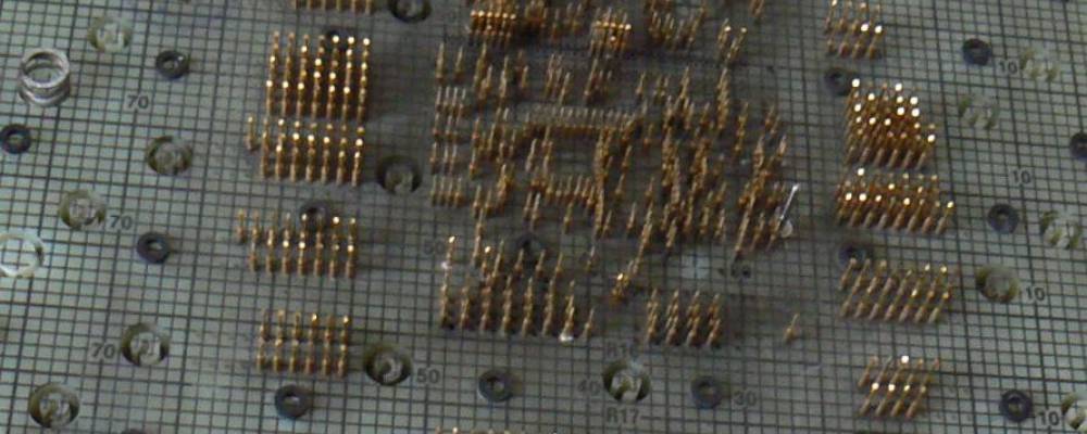
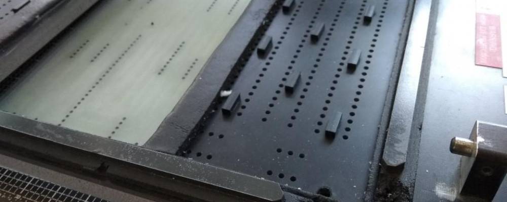
Dirty air in the factory results in contaminants being transported into the fixture. This effect is clearly observable in vacuum fixtures. When a vacuum is applied, environmental air is sucked through the probe clearance holes drilled into the moving plate and into the vacuum pipes. When the vacuum is deactivated the reverse process takes place and airflow into the fixture. In both process dust, abrasive gases or any other pollutant is carried into the fixture and the contaminants end up on the spring probe tips, inside the spring tube housings, on the vacuum fixture seals or on any other fixture component. Even Dust can cause several problems to a fixture. Because of its hydrophilic nature, dust can form a conductive electrolyte film that can compromise the surface insulation resistance of fixture components and increase friction on contact surfaces promoting wear and corrosion. The end effect is a premature degradation and deterioration of the fixture parts.
A similar effect happens when “dirty boards” are tested on the fixture. Dirty PCBs have a considerable amount of flux residue left after soldering usually around the solder joints, but also on vias and test pads, especially when they are close to the components solder joints. When probes contact the board, they break the flux deposit and flux residues detach from the PCB and are drawn into the spring probe tips or inside the spring tube housings. During vacuum on and off, this flux particles can also be deposit on the vacuum fixture seals or on any other fixture component. Flux solder residues can cause severe problems due to aggressive residues they carry, which are corrosive in humid environments. The reason is that the acid part of the flux may not evaporate completely during the soldering process and when they combine with moisture water produce an acid solution that corrodes any material they come in contact with.
Fixture Component deterioration
Test fixtures like any other tooling device will degrade or wear with use. Regular inspection and knowing what to look for will help avoid operation stops or catastrophic failures.
Vacuum Seals
Vacuum seals deteriorate and lose their sealing capacity with use. There are several causes. One possibility is that the seal contacting face was damage after it got in contact with a sharp object. This is often the case with big PCB boards or in fixtures that test several boards. It is not uncommon that the PCB board hits and damages the gate vacuum seal when handling the board in or out of the fixture. The other possibility is that the seal material was damaged. Vacuum seals are especially sensitive to air pollutants and flux solder residues. Their effect on vacuum seals varies from total mechanical destruction to a degradation seal’s material physical characteristics. The vacuum seal shows areas of corrosion or becomes stiff. The last possibility is normal fatigue-like degradation. Over time vacuum seals become brittle or material is removed from the sealing face due to abrasive action.
The existence of a damaged vacuum seal is mainly shown by a leakage sound and a slow vacuum build-up in the fixture. For a good fixture performance, the air in the fixture vacuum chamber should evacuate fast causing a rapid contact between the probes and the PCB. When vacuum leakage occurs, probe pressure on the PCB raises slowly and not to the required level causing poor and intermittent electric contact.
Tooling Pins
In PCB boards with small test pads, accurately positioning the PCB on the test fixture is critical and requires tooling pins matching the PCB’s tolling holes dimension with a very low tolerance. As this tolerance fades, any variation on the position or dimension of the PCB’s tooling holes creates major mechanic stress on the tooling pins. As a consequence tooling pins can be damaged, bent or broken.
Damage tooling pins will affect the fixture target registration accuracy. Registration accuracy depends on an accurate position of the PCB on the fixture. When the tooling pins surface is damaged or wears out, the tolerance between the tooling pins and PCB tooling holes increases modifying the final position of the PCB at the moment that probes contact the target. Tooling pin integrity is key to maintaining the test fixture’s target registration.
Bend or damaged tooling pins will also lead to PCB jamming. As the board is pressed down or released, any cut or mark in the tooling pin surface will obstruct the PCB movement clamping the boar and causing major damages to the PCB.
Pushrods and board stoppers
Pushrods and board stoppers maintain the board in a parallel position and hold it there during the test, but as ware out parts, they are subject to degradation and damage with use.
In the process of designing a fixture, the position of the probe is given by the PCB’s test point layout; push down rods and stoppers are then assembled to stabilize the forces generated by the probes. Their main function is to balance the pressure forces acting on the PCB board to avoid stress areas that may damage the PCB assembly. This balancing function is not only based on a careful distribution of the pushrods and boards stopper through the fixture, but also in their accurate set height.
When push rods and stopper get damage or their surface deteriorate with use, their set height change and their balancing function start degrading to a point where unbalanced pressure forces turn up and the PCB is damaged. There are several causes. Pushrods and board stopper get damage when board components are misplaced or shifted during the welding process and collide with them when the boards are pressed down. A second cause is when they get in contact with dust, air pollutants, and flux solder residues. Pollutant particles can set down on their contact surface destroying the material and changing their set height. Having a fixture designed, manufactured and tested for a stress-free test is worth nothing if missing, damage or wear out push rods or board stoppers are not constantly monitored and replaced.
Test Probe
Probes are ware out parts and as such deteriorate and lose their contacting capacity with use. As the probe hits a hard surface its tip start to degrade until it becomes blunt. A blunt tip has a bigger contact area resulting in weaken contact pressure and reduced ability to penetrate contamination layers. Replacing probes with dull tips is critical for reliable board contact.
Besides the normal ware out process, there are other factors that affect probe degradation:
Contamination on the probe tips and body
In a controlled environment, a probe could last for 1 million cycles before failure, however, in a manufacturing environment, dust, flux, and other contamination can degrade the probe. Solder flux residues, dust and fibrous contaminants from PCB material built up in the valleys and on the tip forming an insulating layer that prevents reliable contact. Typically this degradation is seen as an increase in resistance between the probe and the board under test.
Damage of the internal contact surface
Internal contact surfaces can be damaged by side-loading of the plunger. Side forces affecting the probe during its travel can cause uneven wear of the probe that could eventually deform the probe resulting in a friction force that reduces the working force of the damaged probe. Side-loading can happen when the fixture registration accuracy is compromised by damaged or wear out tooling pins or when contacting open vias or components pins that are displaced from the center.
Photo of a polluted or deformed probe
Contact surfaces can also be damaged by flux residues or fibrous contamination drawn into the probe body. Contamination degrades the probe internal resistance by building oxide on the internal contact surfaces This is critical on fixtures that sit idle for long periods in a humid environment. With less working force the probe will not be as effective in penetrating through oxide layers built on the contact surface.
Conclusion
The main reason for doing fixture maintenance and probe replacement is to maximize the productivity of the test process. As test fixture’s components and probes get damaged or begin to degrade the rate of re-test, false test failures, and worst damaged PCBs due to broken components will increase. These failures will either require time spent retesting the failing boards, time spent on debugging the failures or time spent debugging the fixture or tests. In some cases, the result may be that the tolerance of a test is adjusted to the point that the effectiveness of a test is reduced or disabled. Time spent performing controlled maintenance of the fixture is less than all the ad-hoc re-testing or repairing activities on the line and much less than the damaged a broken fixture can cause to production bottom line.

 22 Sep 2020

